I am an associate professor at the university, this means that I am both a researcher and teacher. I spend half of my time at the university doing research and the other half teaching (there are also several other half devoted to administrative work which makes me sad, but that’s another story).
For the teaching part, I do it at the IUT (Technical Institute) of Saint-Denis in the Sciences and Materials Engineering department. It is a great opportunity because it allows me to work with colleagues who have skills a thousand miles away from mine.
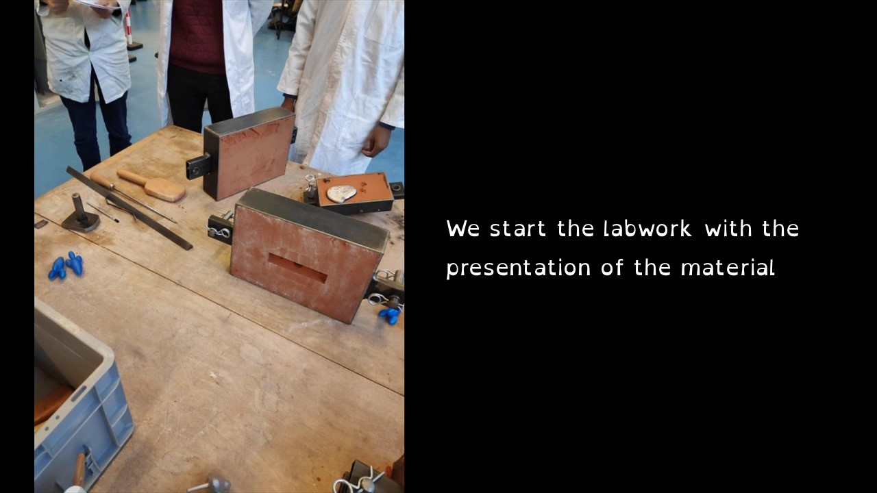
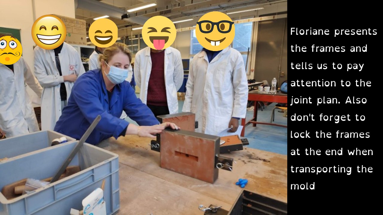
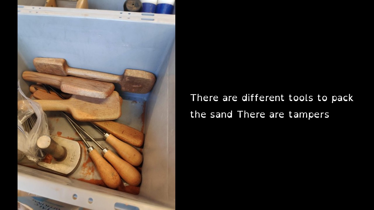
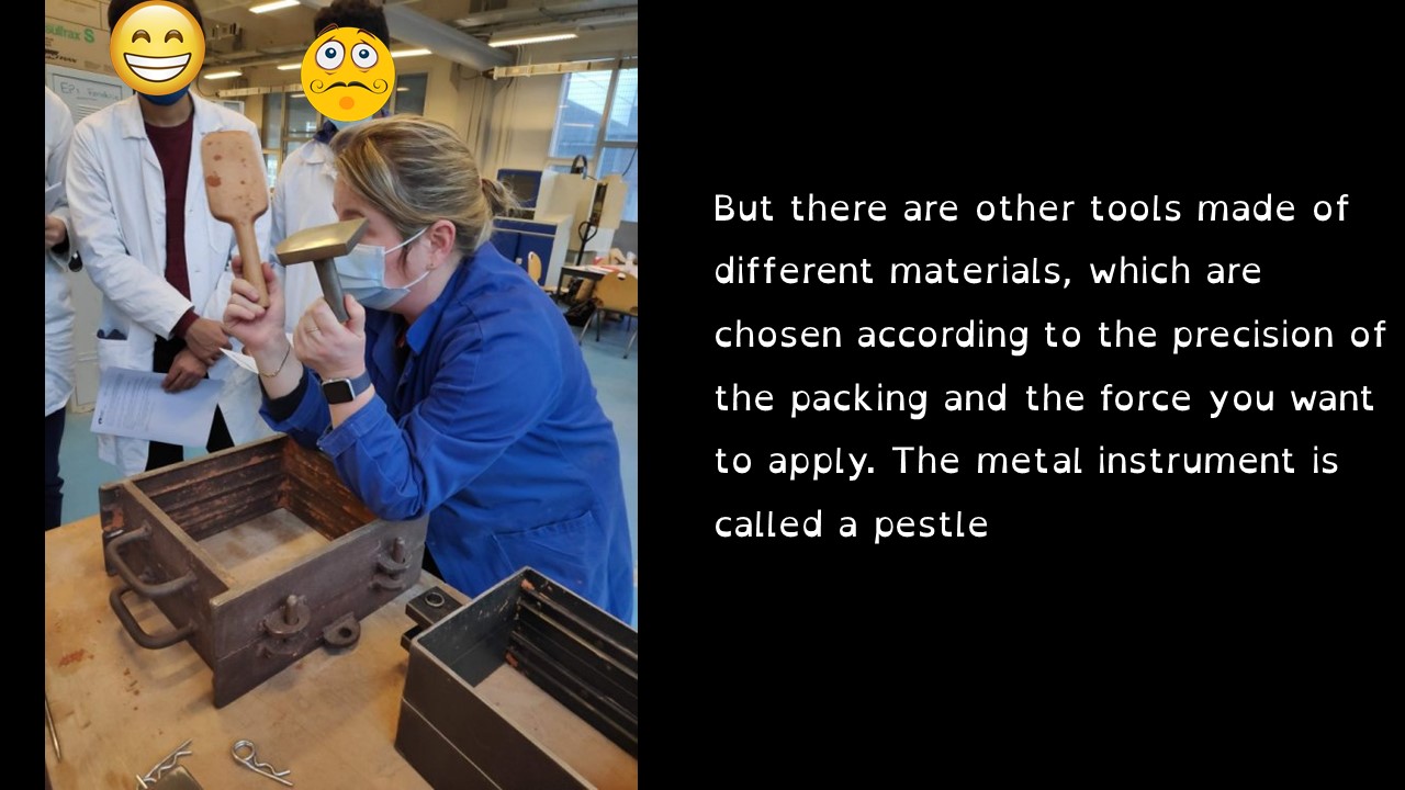
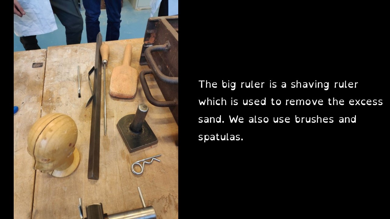
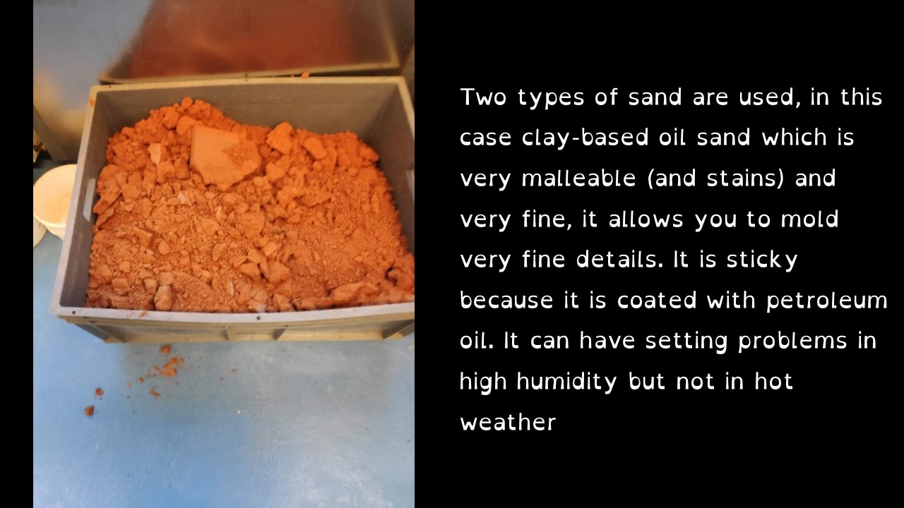
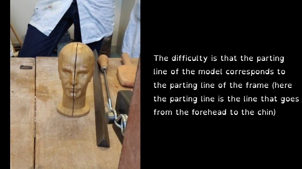
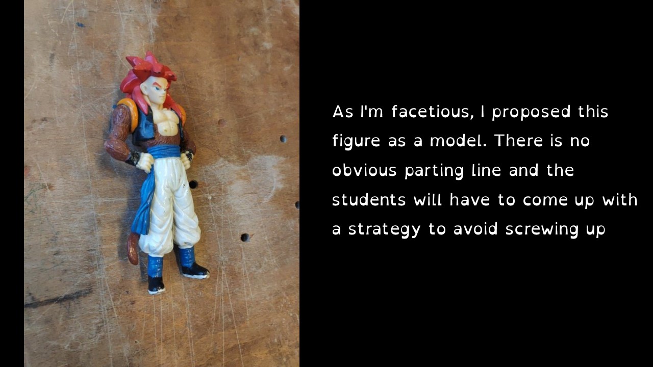
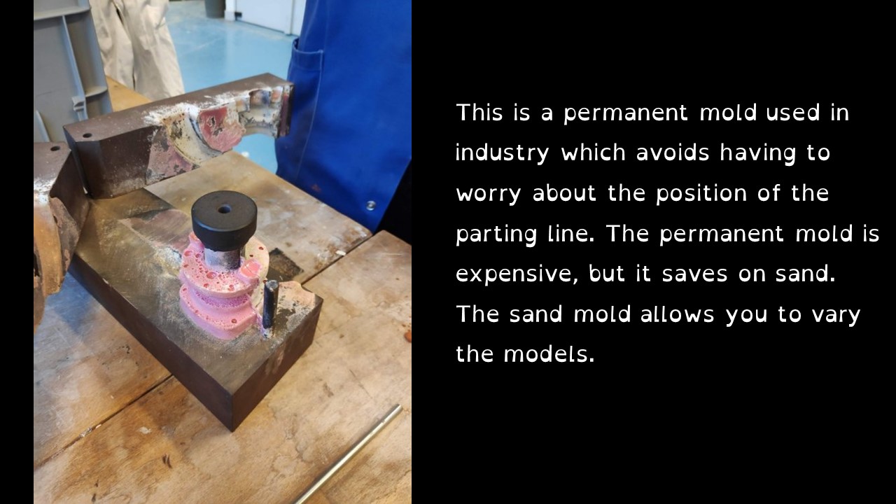
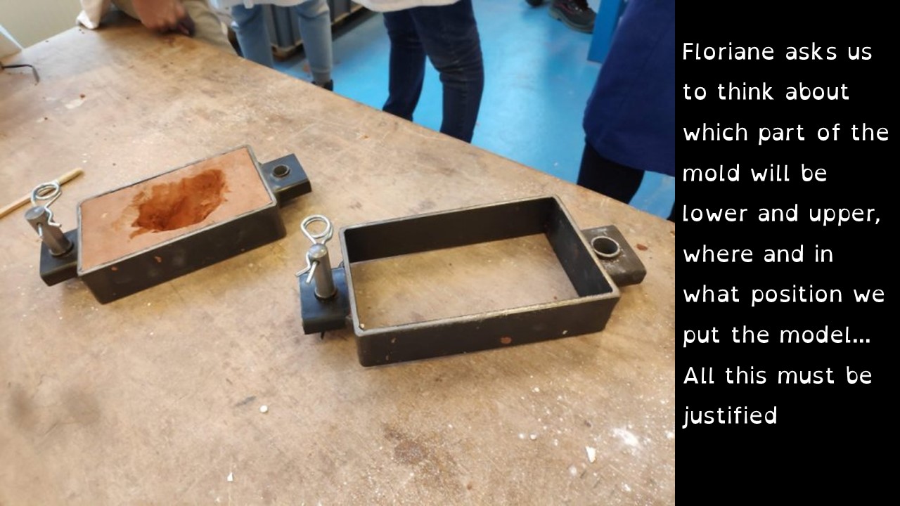
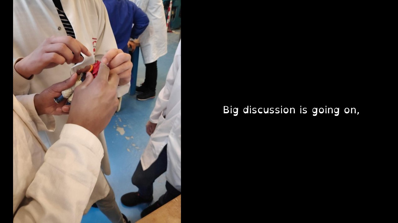
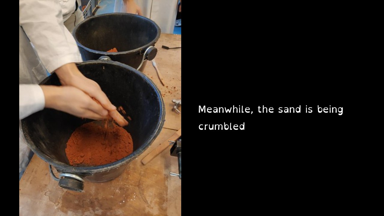
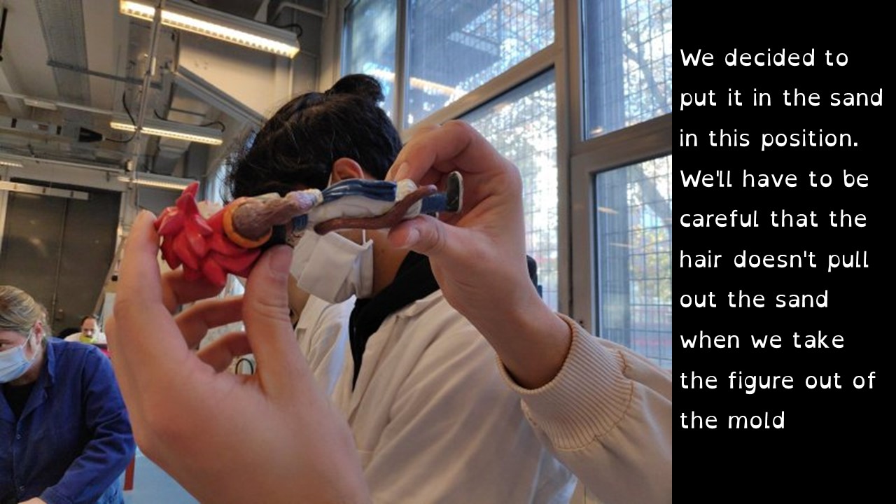
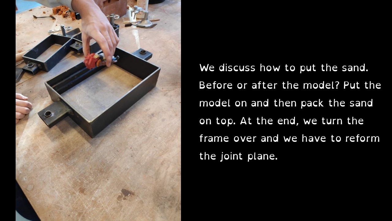
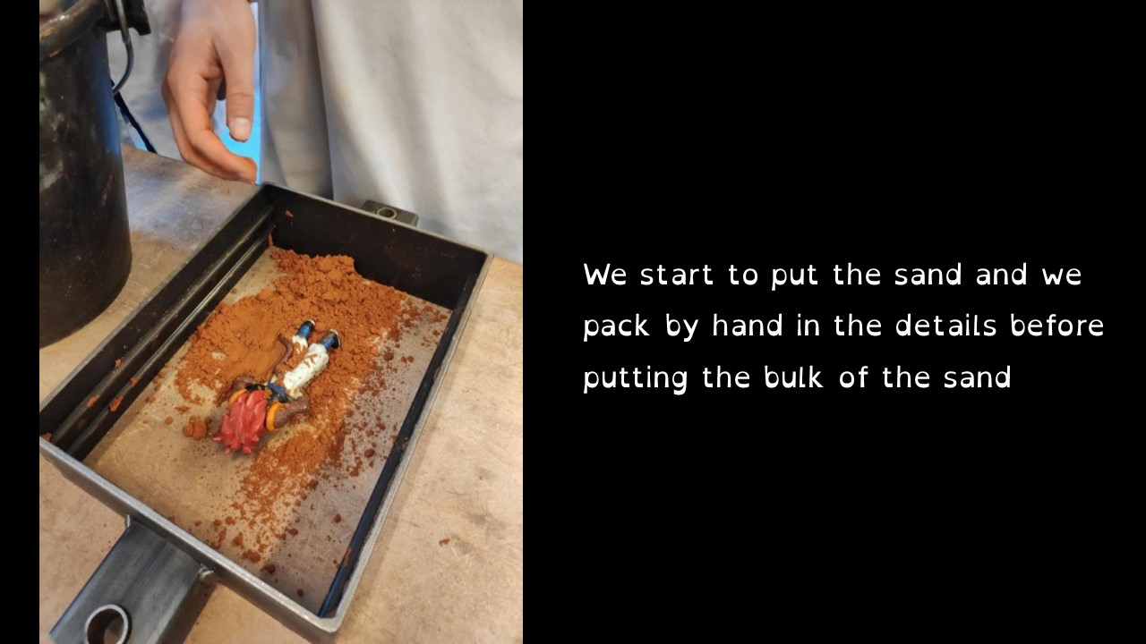
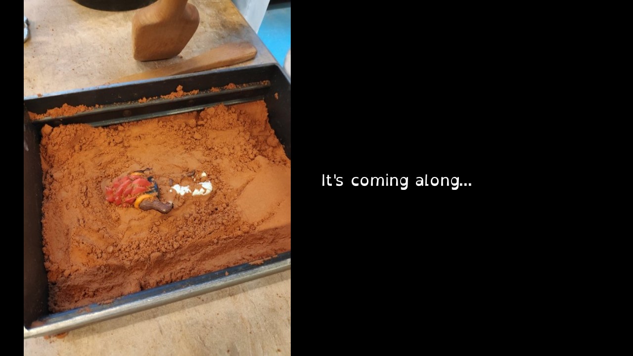
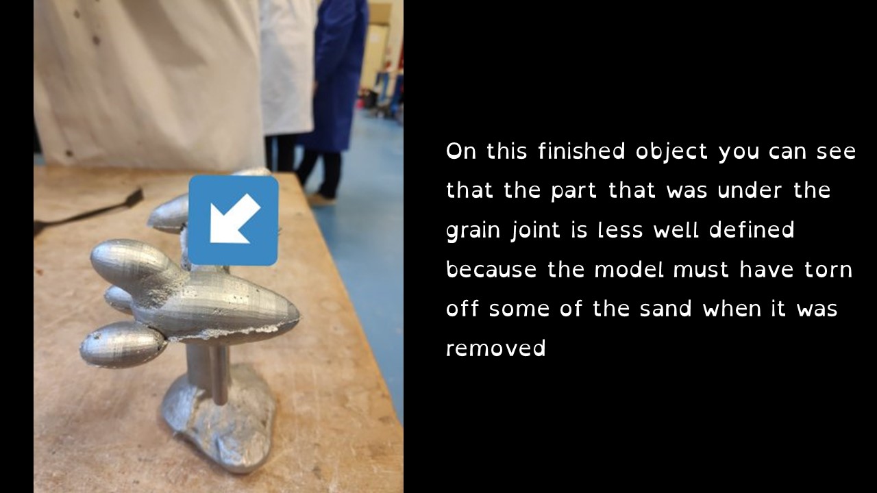
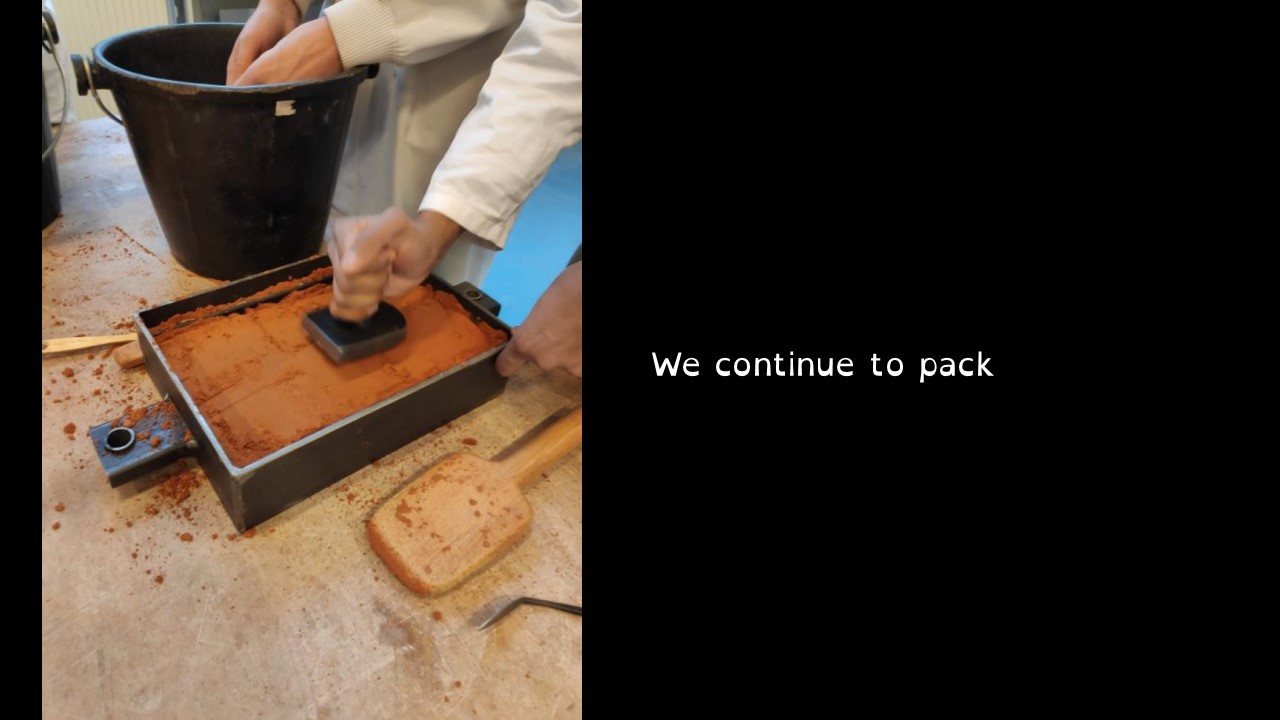
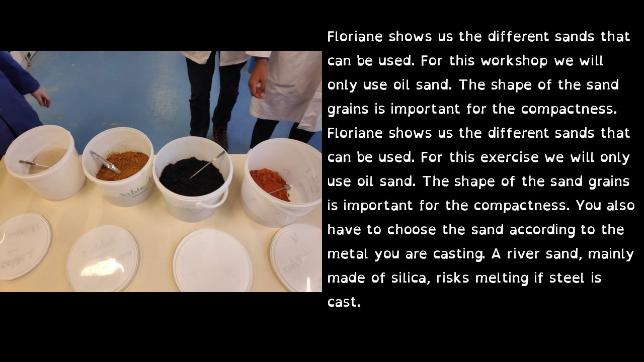
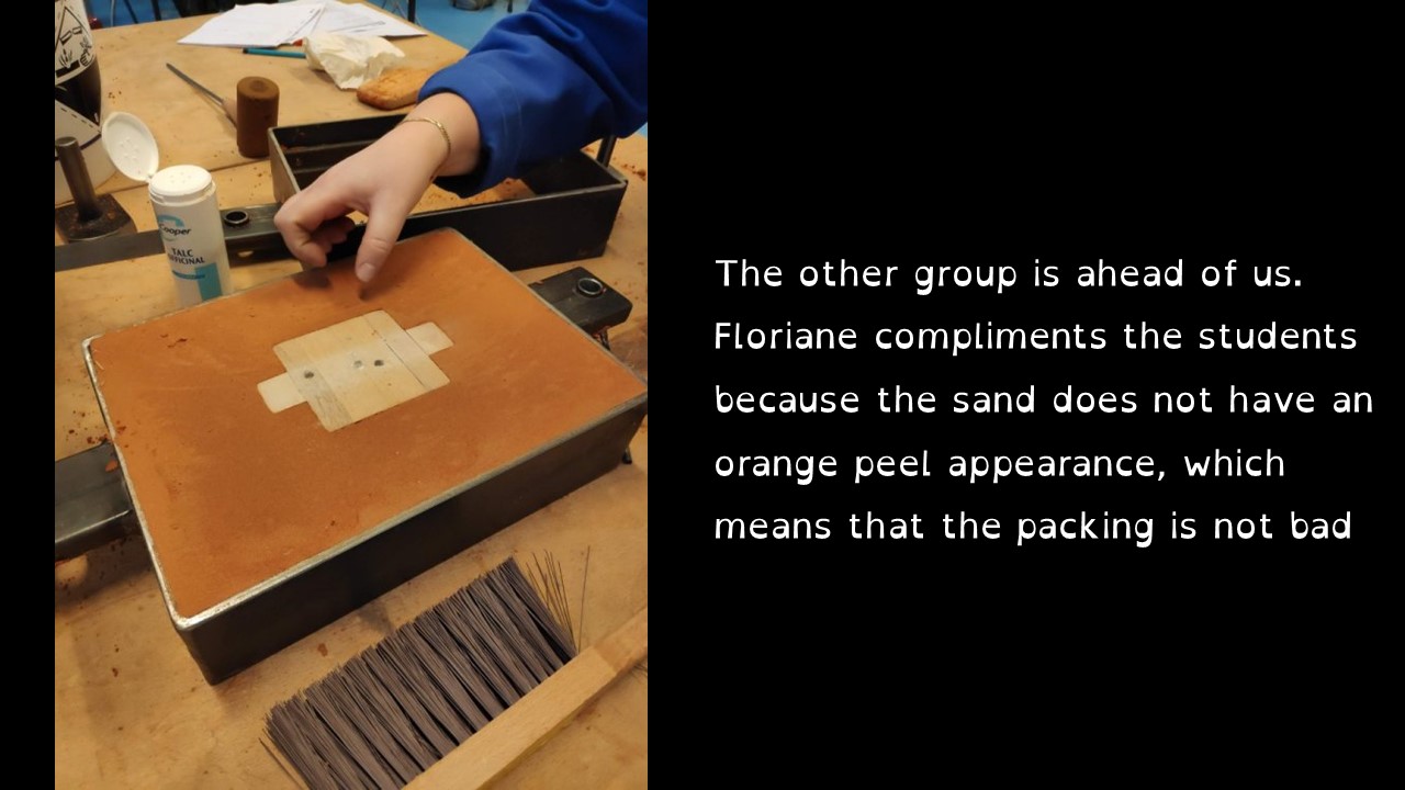
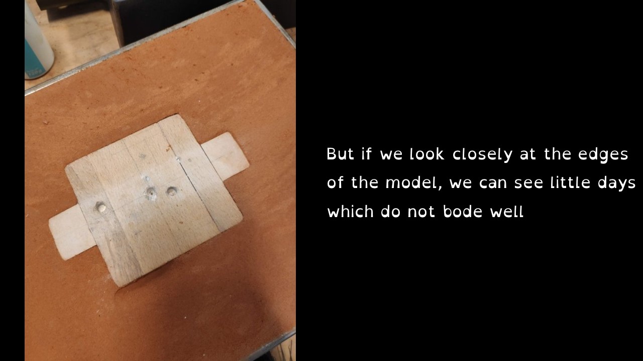
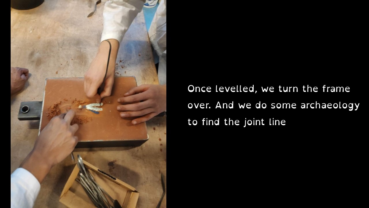
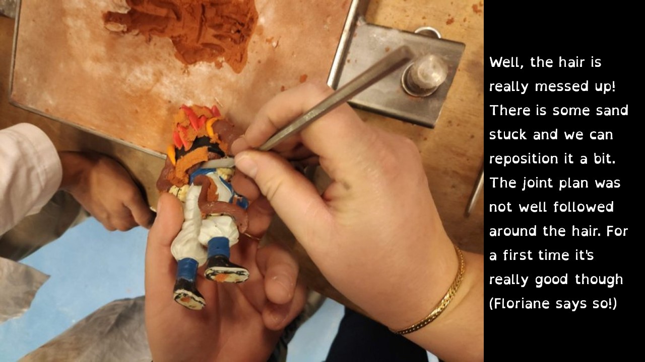
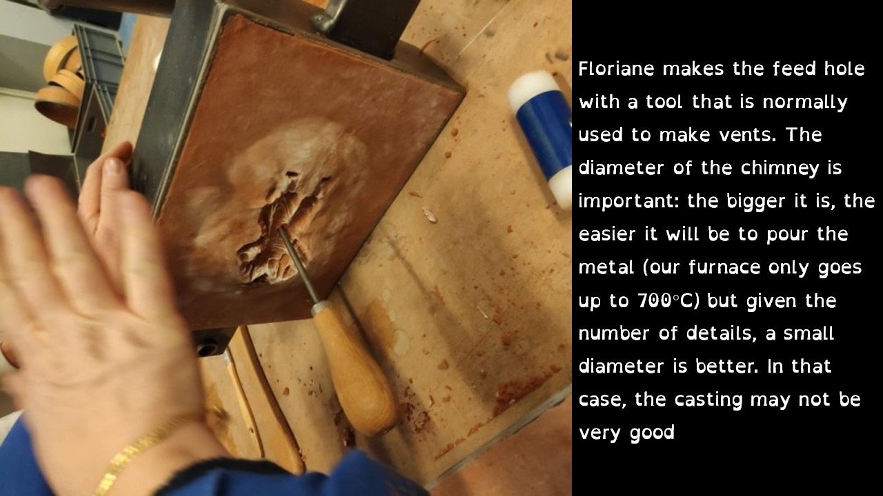
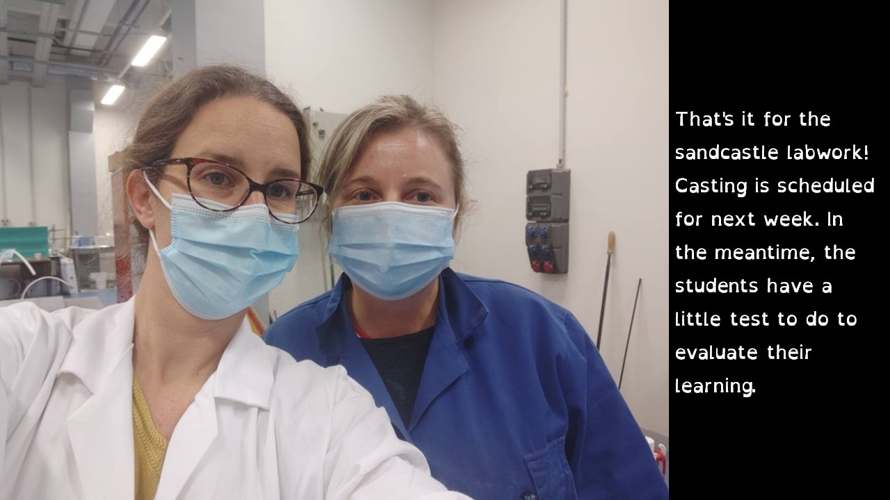
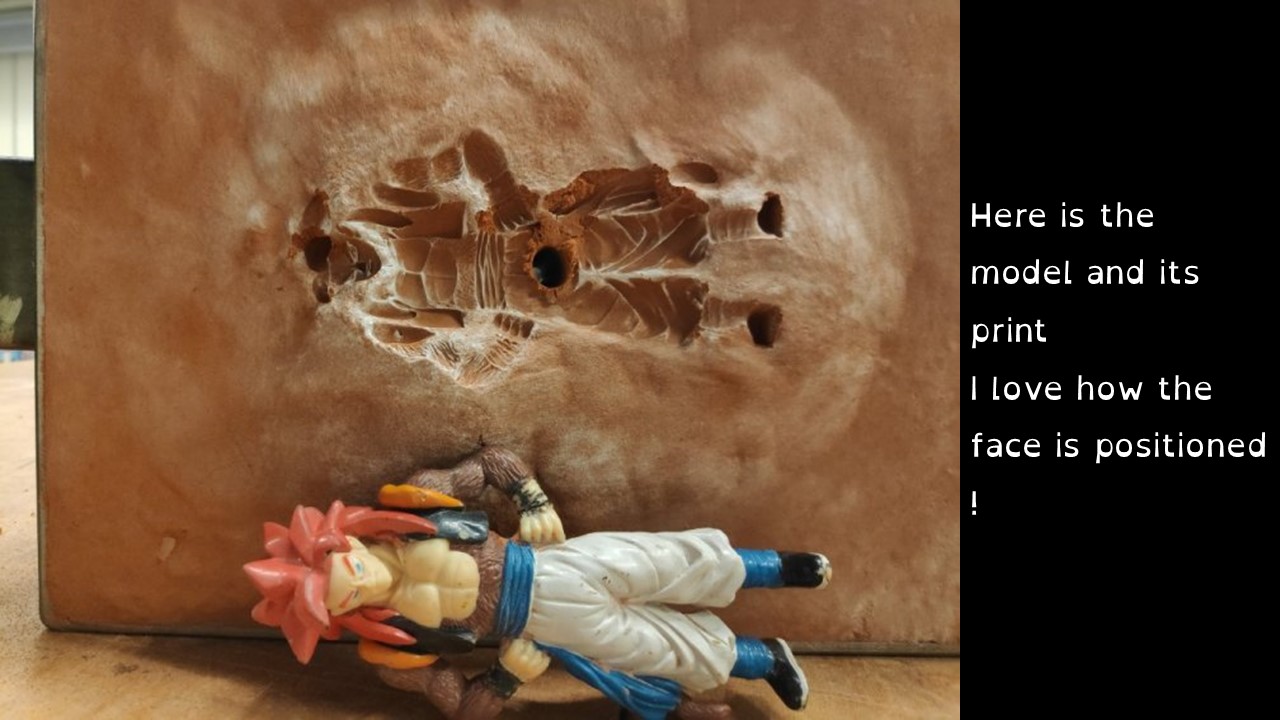
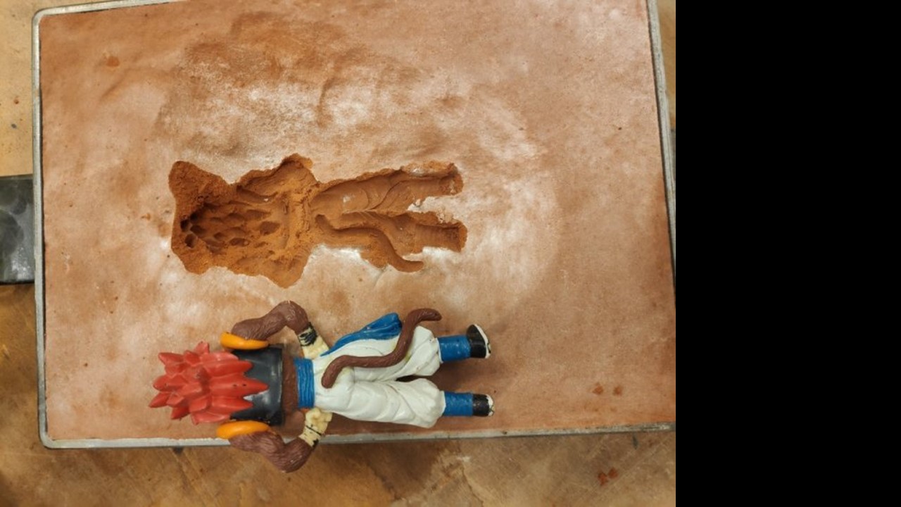
At the end of 2020, my colleague and friend Floriane Laverne allowed me to attend her foundry laboratory. This is a session where students learn how to make a mould into which a metal will be cast. I made a Twitter thread about it at the time that I am happy to share here in a small photo report
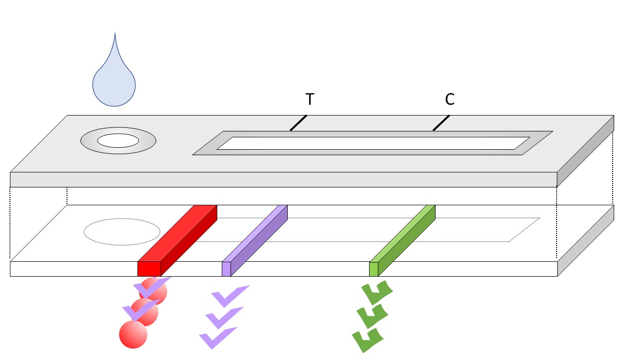
The idea is very simple and I’ll try to describe it with the help of some illustrations: the cotton swab that goes into your nose allows you to collect all the droppings in which the nasty virus aka the antigen would be entangled. Because yes: the test you do at the pharmacy and the one you do at home are exactly the same, the difference is that the pharmacist get the boogers higher up in the nose. By the way “Ag” on top of the test stands for … “Antigen” !
Then, these boogers are mixed with a transparent liquid which has no other purpose than to dilute them. You then put a few drops of the diluted boogers on a piece of filter paper. By capillary action, the liquid will be carried to a first area where there are gold nanoparticles decorated with antibodies.
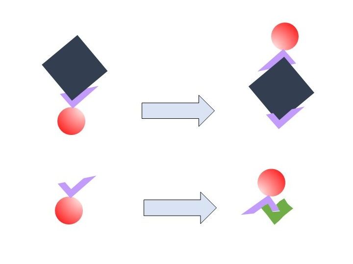
Nanoparticles means that they are tiny, tiny, tiny spheres. At first sight I would say a little less than 100 nm, to give you an idea of how small it is, it is like cutting a hair 100 000 times (I know, it’s not easy to imagine). I’ll come back later on to the role of these nanoparticles. What you need to know is that on these nanoparticles, you find antibodies (red spheres with the purple mark in the sketch) which are molecules capable of specifically “recognising” the virus. When I say “recognise” it is not a mission entrusted to a secret agent, I refer to chemical affinities between the antibodies and proteins on the surface of the virus (the one called spike in this case). So if the virus is in the boogers, we end up with a virus on which many antibodies are stuck and the antibodies are in turn grafted onto nanoparticles. If there is no virus, the antibodies stuck to the nanoparticles remain free.
Meanwhile, the liquid continues to climb in the test and it leaves some kind of red trails: THESE ARE THE NANOPARTICLES!!! This liquid loaded with nanoparticles decorated with antibodies with or without virus will meet two zones:
the first one, noted T for “test”, also contains antibodies against the nasty virus. If, by any chance, a nanoparticle grafted with antibodies that have latched on to the virus passes by, it will be stopped in its tracks and a band will appear .
On the second area, marked C for “clear”, there are again antibodies but these are a bit different, they don’t recognise the virus but the antibodies grafted onto the nanoparticles. If the test works properly, this line should always appear.
There you have it! You know all about self-tests and other antigenic tests performed in pharmacies. Well, no, you don’t know everything. Because there is still one question to be answered: why do these nanoparticles appear red-dish? Gold at the nanoscale is not golden at all, it is red! The first thing to consider is that the light you shine on this self-test is multicoloured. Have you ever seen a rainbow? Well, all those colours are contained in the sunlight. When the light is going to tickle metal nanoparticles, and gold nanoparticles in particular, blue-green light is used to make the electrons oscillate. You have to imagine the blue light as a finger scratching a guitar string. This oscillation of electrons is called a “plasmon” and as it is my speciality, there is a good chance that I will talk about it again on this blog! Anyway, let’s get back to our plasmons. Since the blue-green is used by the nanoparticle, only the red-pink tones remain in the light. And that is what reaches your eyes!
Gold, when it is golden, means that it is present in large quantities and the plasmon is no longer excited in quite the same way. In certain configurations, gold can also appear blue, but I’ll explain another time. Finally, you should know that this story of red gold is as old as glassmaking. The incorporation of gold nanoparticles in glass is described in a 16th century treatise and the greatest glassmakers have used it to make luxurious works.
P.S. Many paper tests work in this way, such as pregnancy tests, which do not react to the presence of an antigen but to a hormone in the urine. The urine is already full of water so there is no need to dilute it and you just have to pee on the test.
That’s all for the booger and pee post, I hope you enjoyed it!
Everyone has heard of atoms. We know they exist, I will tell you another time how we became convinced of their existence. What I can say is that it was in the 19th century and that at that time there was no way to be convinced of their existence by seeing them. This gave rise to many scientific and philosophical disputes (do you have to see something to know that it exists?). Nevertheless, much of the tremendous scientific progress of the 20th century was built on the fact that atoms exist…without anyone having ever seen them.
Today, in the 21st century, can we finally see atoms? If we compare an atom to a sphere, it would have the diameter of a tenth of a billionth of a meter, like a hair that you cut a million times, an ångström if you like… But I imagine that this kind of dimension is not very easy to imagine? Let’s say it’s small enough that no optical microscope is powerful enough to distinguish an atom. So, has anyone ever seen an atom?
The answer is yes, even if “to see” is probably a poor choice of words
To ‘see’ atoms, we can, for example, use a transmission electron microscope (TEM). The principle of an electron microscope is to use electrons instead of light. This microscope is called “transmission” because the electron beam will pass through the material being observed. The first electron microscopes were conceived in the 1930s, notably by Ernst Ruska, who was awarded the Nobel Prize in Physics in 1986 “for his fundamental work in electron optics and for the design of the first electron microscope.” This video (found here) explains how it works
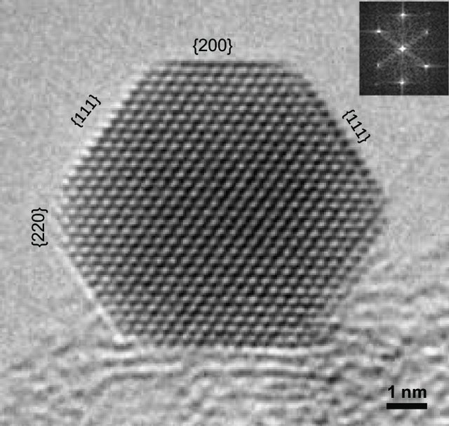
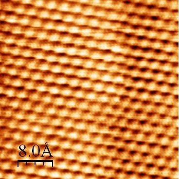
This is a TEM image of a copper (Cu) stack on manganese oxide (MnO). Each small bright spot is an atom. It looks like the MnO atoms are bigger than the Cu atoms… Except that MnO atoms do not exist, there are Mn atoms and O atoms… and it is not possible to distinguish them on this picture
The atoms are so well arranged periodically that when the electrons pass through this material, they undergo a somewhat unusual path. It is said that they have been diffracted. Finally, thanks to the TEM, what we “see” is not the atoms directly but the way they are organised. Above all, with only this image, it is absolutely impossible to say with certainty which atom it is.
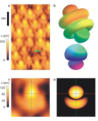
In this picture, the nanoparticle is very structured, with the typical grid pattern of a very good organisation. This organisation is called a crystal. The small numbers between the braces are a notation used in crystallography to identify the orientation of the crystal. However, underneath the nanoparticle there is a kind of fog. This texture shows that there is matter, but as it is disorganised it is no longer possible to distinguish the atoms that compose it.
Another example of a microscope that can “see” atoms is the scanning tunneling microscope (STM). Its principle is to move a tip very close to the surface of the material of interest. The electrical current between the material and the tip is measured, which is a bit special because the tip never touches the surface. The tip is so close (about 1 nanometre) that the electrons have a good probability of passing from the material to the tip! This phenomenon is called the tunnel effect and it depends strongly on the electron supply available in the material.
A short animation on how the STM works is available here
Finally, the STM gives access to the probability of finding an electron at a location. As there are electrons in atoms, it gives an idea of the shape of an atom. For example, here is an image of a gold surface where we can see small organised balls. This image may look like the TEM images, but it does not give the same information at all.
One way to see the difference between STM and TEM is to play with the atoms. Here, we can see 48 iron atoms on a copper surface. The interaction of the electrons of each of the atoms causes these kind of circles in the water and this crown of mountains that we call quantum corral. The density of electrons is greater on the iron atoms, so that they no longer look spherical at all!
Finally, here is one of the scientific images that I find most extraordinary.
It is still in STM and it has been published a few years ago. These images are exceptional because we can see strangely shaped atoms. In reality, this is not the case. We know for decades now that electrons do not revolve around the atomic nucleus as in a planetary system. Electrons are both waves and particles that describe orbits of various shapes. The equations of quantum mechanics can simulate these shapes, but no one had yet obtained experimental proof until then.
There are a few other techniques that allow us to “see” atoms, but you can now understandd that the word “see” is not at all appropriate. The training and experience of physicists allow them to see beyond the raw image. This insight is the very first step in the analysis of the results that will allow us to understand a little bit more how matter is formed.
A nanometre is one billionth of a metre, a hair cut 100,000 times, in short, it’s so small that you can’t see it or feel it. Yet nano is made all day long all over the world. Nano is all around us. As I write these words, I am using my computer, whose processor and screen are full of nano or micrometer sized objects. How can we make such small things in a controlled way?
There are many ways to do this, but today I’m going to talk about a process called lithography.
This is a technique that kindergarten pupils know well: stencilling. With illustrations it will be easier, so here is what a lithography process is.
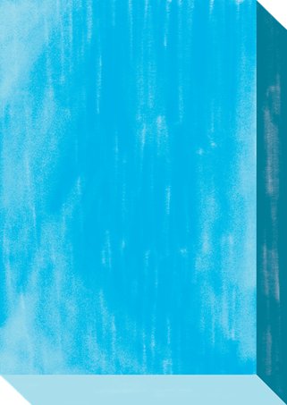
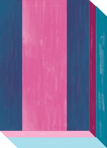
It all starts with the support on which the nano-object is to be fabricated. This support is often called “the substrate” in our jargon. It is chosen for its physical and chemical properties (transparent, conductive, hydrophobic, etc.). For us, here it will be this blue rectangular plate (it can represent glass, silicon, etc)
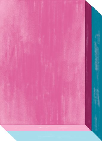
A lithography process starts by depositing a resist (here in pink) on the substrate. A resist is a slightly viscous liquid which has particular properties: UV light modifies its molecular structure! To deposit it, a few drops are poured onto the substrate and the whole thing is spun at several thousand rotation per minute. This step is called “spin-coating“.
Now comes the stencil stage! Except that in our jargon we don’t call it a stencil but a mask (yes, that’s not really jargon ;-)). The idea is that some parts are opaque and others transparent to light. The shape of the openings of this mask is the pattern that we want to reproduce. Here we have chosen a line, but it can be any shape!
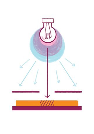
Once the mask has been placed, the whole [mask – resin – substrate] is illuminated with UV light. This light has been chosen to change the molecular structure of the illuminated resist. A more rigorous way of saying this is that the wavelength of the light allows the polymer that makes up the resist to cross-link.
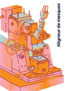
A mask aligner is used to illuminate the resin – we call it “insolation“. This instrument allows the mask to be positioned correctly in relation to the substrate, but also to be pressed against the resist to avoid shadow effects. Above all, it allows the duration of the exposure to be controlled.
Since the beginning, I have been trying to explain how to make nano-objects. But what I have described so far – optical lithography – is more about making micro-objects. If you want to go to the nano scale (1,000 times smaller), you will use a very similar technique but where the light and the mask are replaced by an electron beam. The mask aligner is then replaced by a scanning electron microscope (SEM) whose electron beam is used like a brush to draw the desired pattern on an electro-sensitive resin
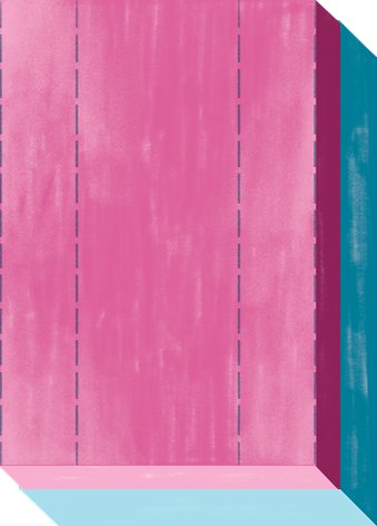
Let’s get back to the point! Once it is exposed, the molecular structure of the exposed resist is no longer the same as that of the masked resist. This is important because the exposed resist can be dissolved in a liquid called a developer. In fact, the sample is dipped in a beaker and when it comes out the exposed part will have been dissolved.
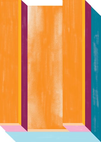
And here it is! A very small opening (micro for optical lithography and nano for electronic lithography) has been made in the resist… The lithography itself stops here, but making holes in the resist is not very interesting, so here are the two steps that can follow.
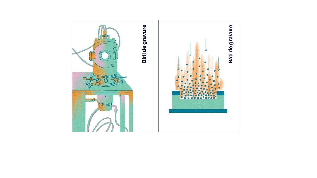
1 If the objective is to make trenches in the substrate. It is then necessary to dig, i.e. to remove material. For this purpose, an etching frame is used, for example. This is an enclosure in which it is possible to control the pressure and the gases present. The idea is to precipitate this gas against the sample to remove material either by an abrasion effect or by chemical reaction with the surface
At the end of this step, the substrate has been etched but there is also some resist left. To dissolve it, it is simply soaked in a beaker filled with acetone.
And here is a nano- or micro-trench made on the substrate!
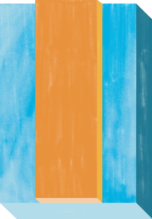
2 Another possibility is to make a relief structure on the substrate. We therefore seek to add material. Here again, there are different techniques available. One of the most common is evaporation. The sample is inserted in an instrument very similar to the etching instrument in that the pressure and gases present are very finely controlled. The difference is that there is also a metal heated sufficiently for it to evaporate. The sample is placed in this atomic vapour and is soon completely covered.
The evaporated material covers both the substrate and the resist residue. Here again, the sample is soaked in a beaker of acetone to dissolve the resist. This operation is called “lift-off“.
And here is a gold nano- or micro-wire made on the surface of the substrate!
Now you know how to make objects without seeing and handling them! I hope that these superb illustrations by Clara Hinoveanu have helped you to understand. The images are taken from a project I did with the “physics reimagined” team: the nano factory, which you can find here
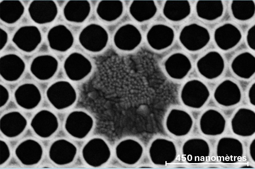
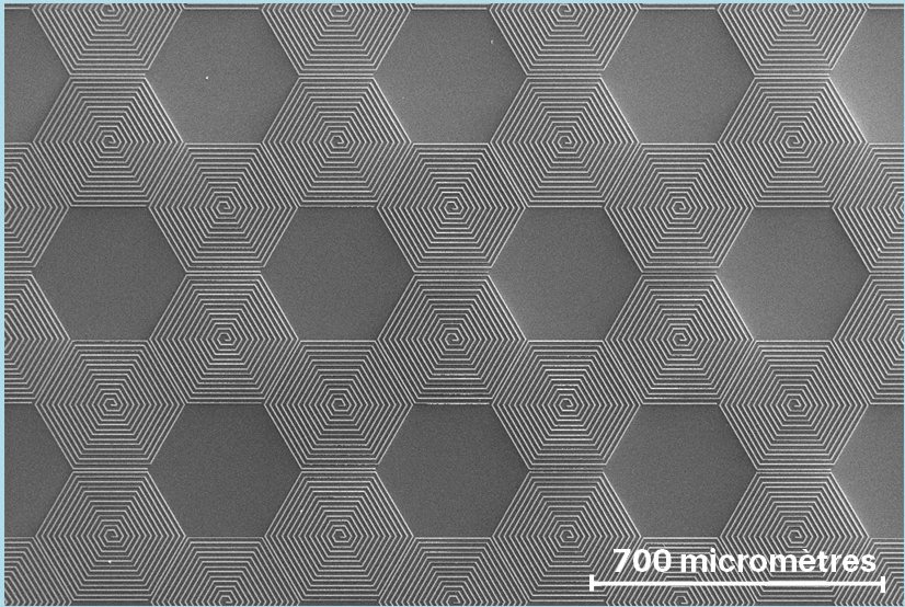
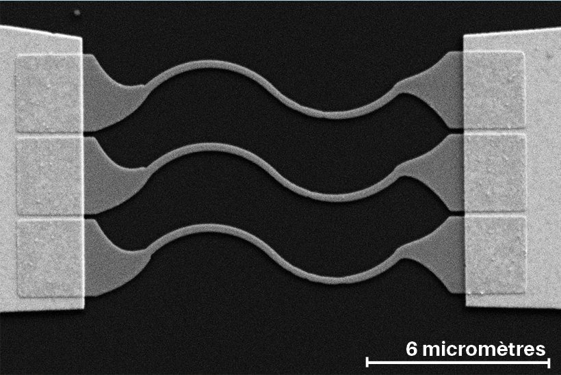
To finish, and to show you how powerful these techniques are, here is a small gallery of objects made by lithography
Quantum boxes with carbon nanotubes Richard Deblock, LPS, Université Paris Saclay – CNRS
Honeycomb network of superconducting resonators Alexis Morvan, LPS, Université Paris Saclay – CNRS
Contacted magnetic nanopists, Jean Yves Chauleau, LPS, Université Paris Saclay – CNRS
Post Scriptum
For those of you who arrived here by seeing a short video of me dressing in a blue suit, you may be wondering what this has to do with anything. Lithography means making objects that are so small that they are smaller than the cells in our skin, the diameter of our hair and even the threads in the fabric of our clothes. If one of these dusts were to fall on our sample, that would be the end of nanos!
This is why nano- and micro-fabrication is done in a so-called clean environment where the number and size of dust is controlled. It is required to dress in a suit to avoid spreading dust in the clean room facility.